Research · Publication & note
Silicon colloids: A new enabling nanomaterial - Notes
Research publication
Published abstract
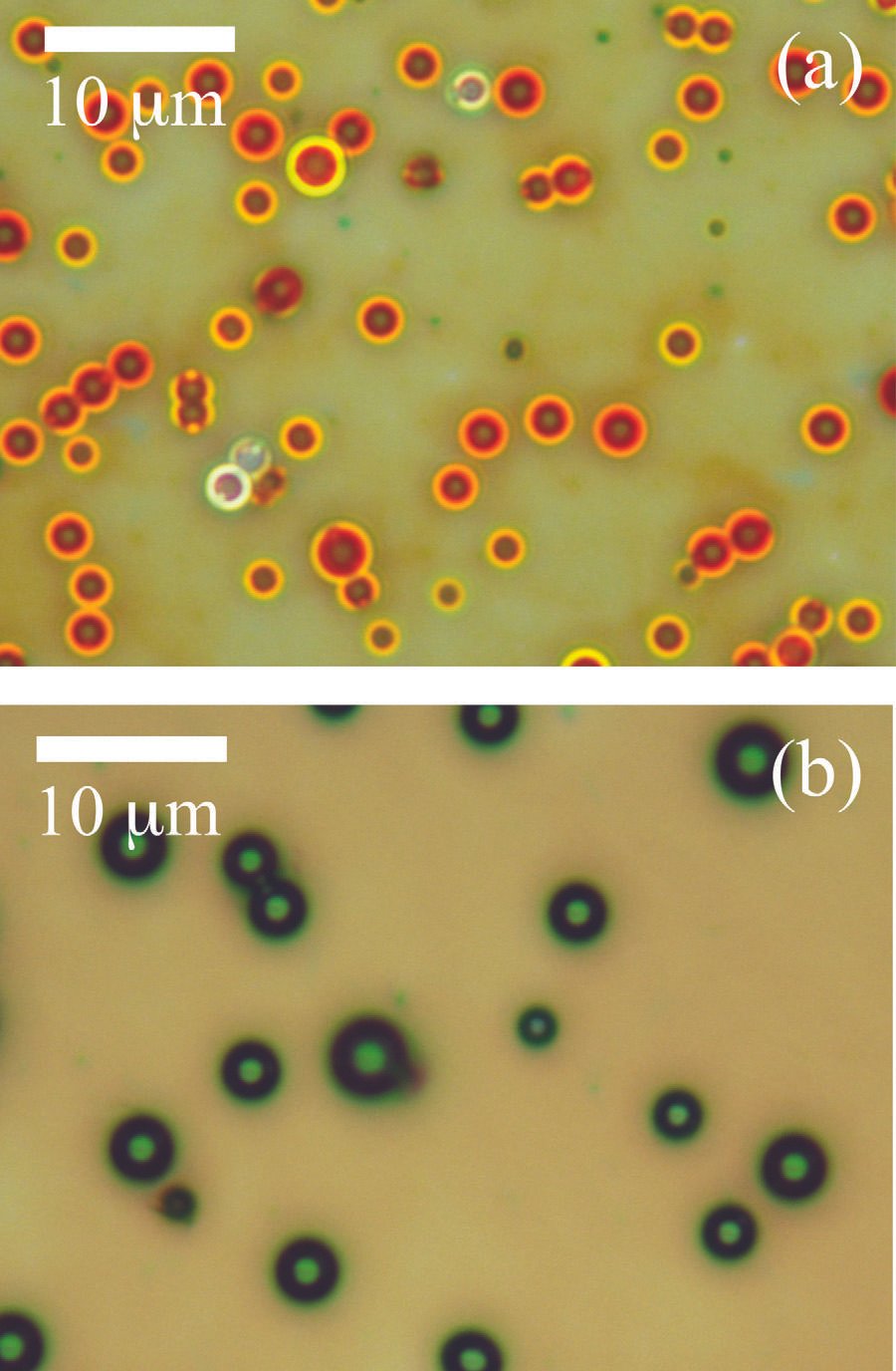
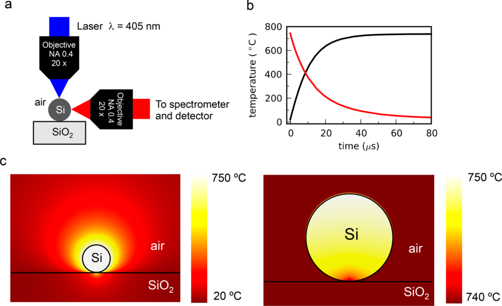
We have recently developed a new type of silicon structure that we refer to as a silicon colloid. This new material consists of almost perfectly spherical silicon micro- and nanoparticles with a very smooth surface. They are able to trap light very efficiently in a large-span frequency range covering the visible to the far infrared regions. Silicon colloids can be thought of as a completely new material for scientific and technological purposes, with manifold applications covering electronics, photonics, cosmetics, or paints, among others. Here, we report on the synthesis of polycrystalline, amorphous, and porous silicon colloids, as well as their optical properties, some applications concerning light filters, and photonic bonding.
Figures
Source: F. Meseguer et al., J. Appl. Phys. 109, 102424 (2011). © American Institute of Physics.
Source: F. Meseguer et al., J. Appl. Phys. 109, 102424 (2011). © American Institute of Physics.
Source: F. Meseguer et al., J. Appl. Phys. 109, 102424 (2011). © American Institute of Physics.
Source: F. Meseguer et al., J. Appl. Phys. 109, 102424 (2011). © American Institute of Physics.
Source: F. Meseguer et al., J. Appl. Phys. 109, 102424 (2011). © American Institute of Physics.
Source: F. Meseguer et al., J. Appl. Phys. 109, 102424 (2011). © American Institute of Physics.
How to cite
Article access and reuse
This is a subscription article. No publisher PDF is hosted. Figures are shown with full citation on an author's personal, non-commercial website; the definitive AIP article is linked above.
Related publications

Research fields
Bottom-up
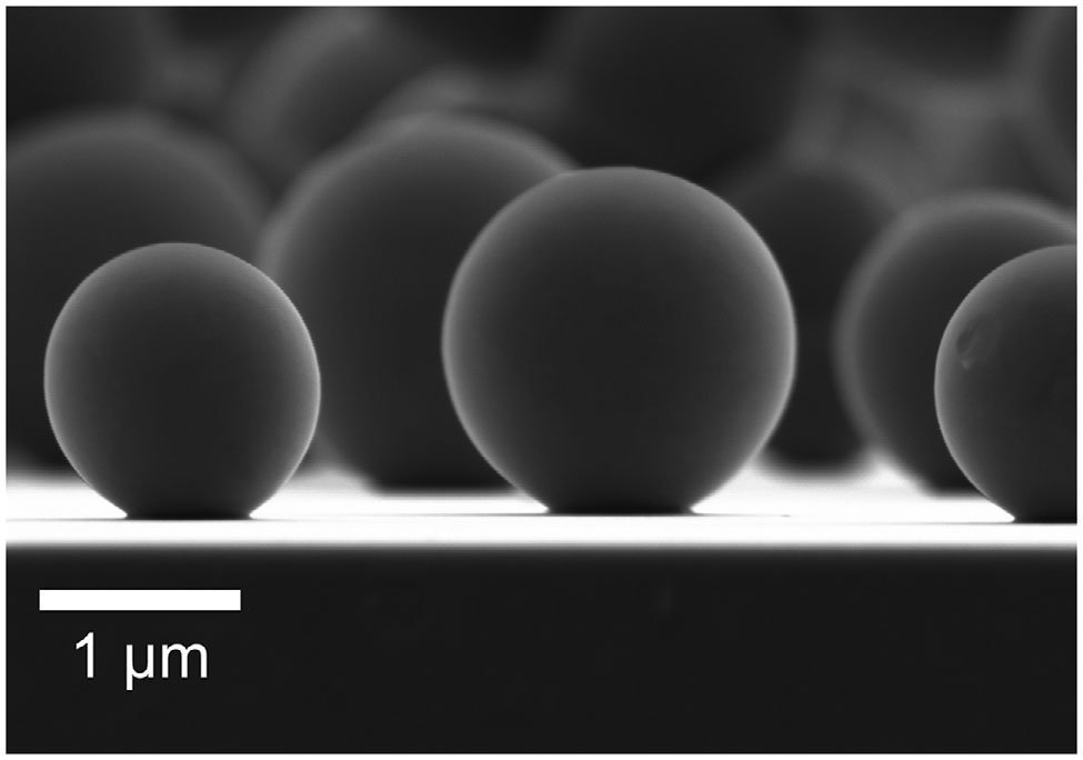
Gas-phase disilane decomposition yields amorphous, polycrystalline or porous silicon microspheres whose density and surface chemistry permit handling as colloids. Their high refractive index adds strong Mie confinement to a particle platform otherwise compatible with solution assembly.
Simulations & fits
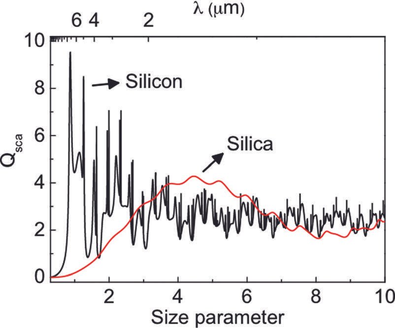
Mie-scattering calculations compare silicon and silica spheres and relate resonant efficiency to particle diameter and refractive index. Spectral fits provide an optical route to identify individual colloids and evaluate their potential as microcavities.
Characterization
Optical and electron microscopy, infrared spectroscopy, scattering and transmission measurements distinguish the silicon allotropes and their conversion under heat or oxidation. The combined evidence connects chemical composition, morphology and resonant optical behaviour.
RESEARCH TOPICS
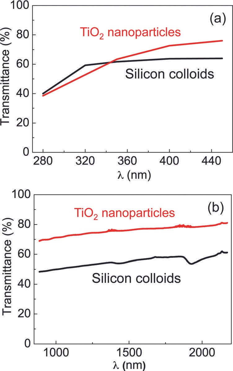
 EmissionThe paper also tests a macroscopic consequence: surfaces coated with a 1% silicon-colloid sunscreen are compared with uncoated surfaces under a xenon lamp to evaluate heating by ultraviolet, visible and infrared radiation. Emission and scattering are therefore connected to a practical spectral-filtering function rather than described only as colour.
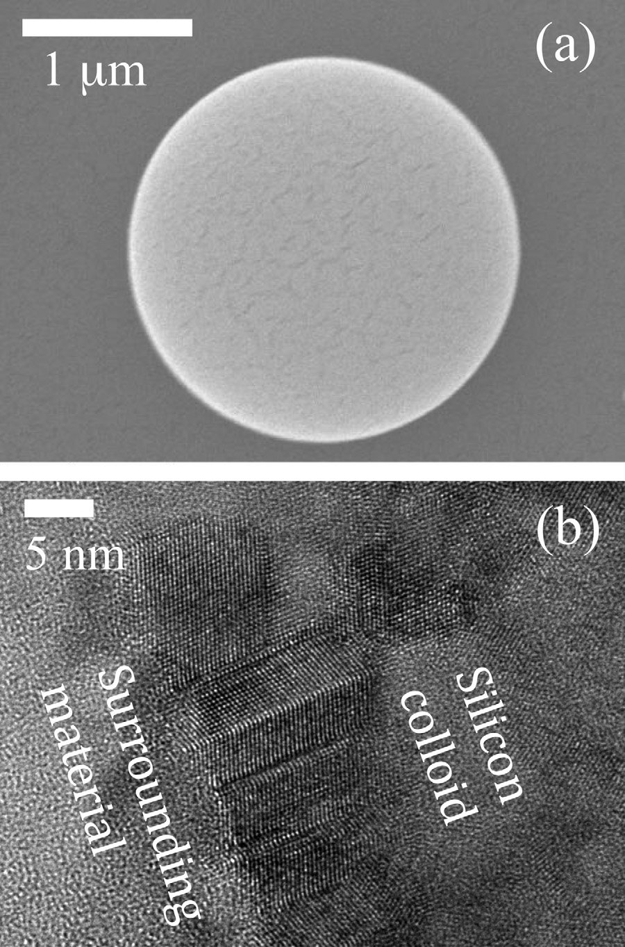
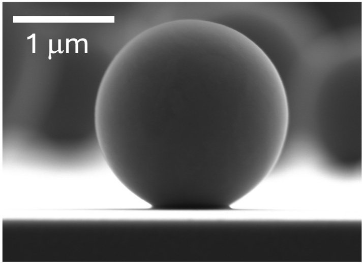
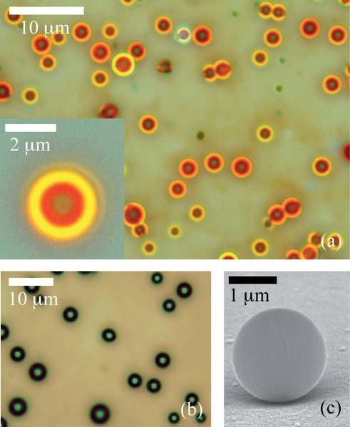
 MaterialsDisilane decomposition creates spherical silicon particles through gas-phase nucleation and surface-tension-driven growth. Figure 3 shows a representative polycrystalline sphere formed after a five-minute decomposition and anneal, tying its optical modes to a documented processing history.
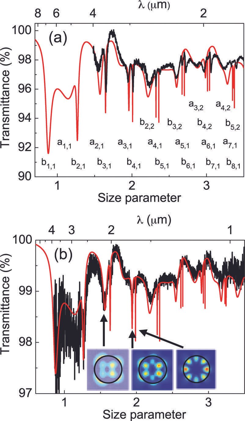
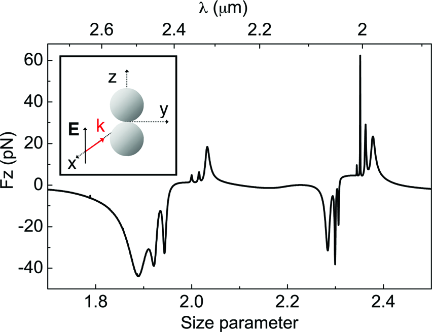
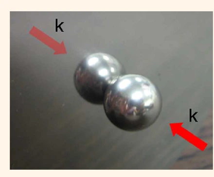
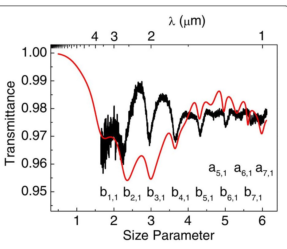
 ResonatorsIndividual spheres are measured by Fourier-transform infrared transmission and display TE- and TM-like Mie resonances whose positions depend on diameter and refractive index. The paper also models paired spheres, showing optical bonding and antibonding combinations analogous to coupled atomic states.
 ChemistryThis chemistry controls absorption, refractive index and visible appearance: longer-grown amorphous spheres look black because silicon absorbs visible light, whereas porous and annealed particles scatter strongly. The chemical route is therefore inseparable from the photonic response attributed to the final colloid.