
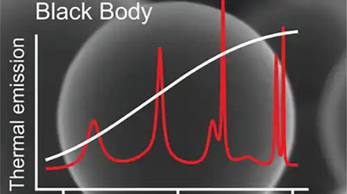
Silicon microspheres with a diameter in the range of 2–3 micrometers constitute photonic nanocavities that emit light through their Mie resonances when heated at high temperatures. At 500–600 °C these microresonators show a particular mid-infrared (MIR) emission dominated by the lowest order modes. Such resonances feature a large free spectral range, about 600 cm−1, and a high proximity to the critical coupling condition. In fact, resonances with high-quality factor, around 160 are found. It corresponds to the limit of detection of their measuring setup, being 600 the theoretical value. Most importantly, several modes emit light above the calculated black body limit because they feature an optical absorption cross-section larger than their geometric one. All these characteristics set silicon microspheres as very promising zero-dimensional materials for developing micrometric and sub-wavelength light sources in the MIR.

Supporting information with additional figures and explanations.

Magnetic 2D materials hold promise to change the miniaturization paradigm of unidirectional photonic components. However, the integration of these materials in devices hinges on the accurate determination of the optical properties down to the monolayer limit, which is still missing. By using hyperspectral wide-field imaging we reveal a non-monotonic thickness dependence of the complex optical dielectric function in the archetypal magnetic 2D material CrI3 extending across different length scales: onsetting at the mesoscale, peaking at the nanoscale and decreasing again down to the single layer. These results portray a modification of the electronic properties of the material and aligns with the layer-dependent magnetism in CrI3, shedding light into the long-standing structural conundrum in this material. The unique modulation of the complex dielectric function from the monolayer up to more than 100 layers will be instrumental for understanding and manipulating the magneto-optical effects of magnetic 2D materials.

We make use of a phase-sensitive set-up to study the light transmission through a coupled waveguide-microdisk system. We observe a splitting of the transmission resonance leading to an unbalanced doublet of dips. The experimental data are analyzed by using a phasor diagram that correlates the real and the imaginary parts of the complex transmission. In addition, detailed features are evidenced by a complex inverse representation of the data that maps ideal resonances into straight lines and split resonances into complicated curves. Modeling with finite element method simulations suggests that the splitting and the unbalance is caused by an induced chirality in the propagation of the optical fields in the microdisk due to the interplay between the stochastic roughness and the intermodal dissipative coupling, which yield an asymmetric behavior. An analytical model based on the temporal coupled mode theory shows that both a reactive and a dissipative coupling of the counter-propagating modes by the surface roughness of the ring resonator are required to quantitatively reproduce the experimental observations and the numerical simulations.

We study light transmission and reflection from an integrated microresonator device, formed by a circular microresonator coupled to a bus waveguide, with an embedded S-shaped additional crossover waveguide element that selectively couples counter-propagating modes in a propagation-direction-dependent way. The overall shape of the device resembles a “taiji” symbol, hence its name. While Lorentz reciprocity is preserved in transmission, the peculiar geometry allows us to exploit the non-Hermitian nature of the system to obtain high-contrast uni- directional reflection with negligible reflection for light incident in one direction and a significant reflection in the opposite direction.
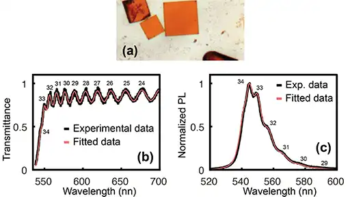
A precise knowledge of the optical properties, specifically the refractive index, of organic/inorganic perovskites, is essential for pushing forward the performance of the current photovoltaic devices that are being developed from these materials. Here we show a robust method for determining the real and the imaginary part of the refractive index of MAPbBr3 thin films and micrometer size single crystals with planar geometry. The simultaneous fit of both the optical transmittance and the photoluminescence spectra to theoretical models defines unambiguously the refractive index and the crystal thickness. Because the method relies on the optical resonance phenomenon occurring in these microstructures, it can be used to further develop optical microcavities from perovskites or from other optical materials.
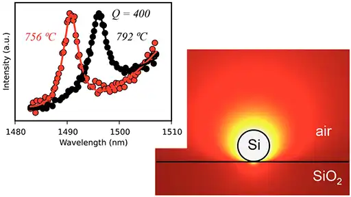
Planck’s law constitutes one of the cornerstones in physics. It explains the well-known spectrum of an ideal blackbody consisting of a smooth curve, whose peak wavelength and intensity depend on the temperature of the body. This scenario changes drastically, however,
when the size of the emitting object is comparable to the wavelength of the emitted radiation. Here we show that a silicon microsphere (2−3 μm in diameter) heated to around 800 °C yields a thermal emission spectrum consisting of pronounced peaks that are associated with Mie resonances. We experimentally demonstrate in the near-infrared the existence of modes with an ultrahigh quality factor, Q, of 400, which is substantially higher than values reported so far, and set a new benchmark in the field of thermal emission. Simulations predict that the thermal response of the microspheres is very fast, about 15 μs. Additionally, the possibility of achieving light emission above the Planck limit at some frequency ranges is envisaged.

High refractive index nanowires are very attractive because of their waveguiding properties and their multiple applications. In this sense, metal halide perovskites, an emerging and appealing optoelectronic material, have also been tailored into nanowire structures. Here, we present an easy, low-cost and versatile method that has made possible to achieve nanowires of controlled and uniform width. The method has been applied here to all-inorganic and hybrid lead bromide perovskite (CsPbBr3 and CH3NH3PbBr3 respectively) materials. The procedure is based on the spin coating of precursor solutions, at room temperature, on a PDMS replica of the periodic grooves and lands of commercially available Compact Disc (CD) or Digital Versatile Disc (DVD) polycarbonate plates. The method can be applied for the synthesis of other material nanowires before being transferred onto other substrates. The obtained CsPbBr3 and CH3NH3PbBr3 nanowires exhibit high photoluminescence and guiding light properties along the material.
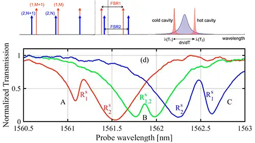
We report on the modeling, simulation, and experimental demonstration of complete mode crossings of Fano resonances within chip-integrated microresonators. The continuous reshaping of resonant line shapes is achieved via nonlinear thermo-optical tuning when the cavity-coupled optical pump is partially absorbed by the material. The locally generated heat then produces a thermal field, which influences the spatially overlapping optical modes, allowing us to alter the relative spectral separation of resonances. Furthermore, we exploit such tunability to continuously probe the coupling between different families of quasi-degenerate modes that exhibit asymmetric Fano interactions. As a particular case, we demonstrate a complete disappearance of one of the modal features in the transmission spectrum as predicted by Fano [Phys. Rev. 124, 1866 (1961)]. The phenomenon is modeled as a third-order nonlinearity with a spatial distribution that depends on the stored optical field and thermal diffusion within the resonator. The performed nonlinear numerical simulations are in excellent agreement with the exper- imental results, which confirm the validity of the developed theory.
We report on the observation of optical bistability in an integrated planar microresonator with embed-ded silicon nanocrystals (Si-ncs). The phenomenon originates from the thermo-optical modulation of the silica-embedded Si- ncs refractive index, which in turn alters the spectral position of the resonator mode. The estimated thermo- optical coefficient of the Si nanocrystalline material, dn/dT ≈ 2.92 × 10⁻⁵ K−1, is an order of magnitude lower than that of bulk silicon. Both time-resolved pump-and-probe experiments and numerical simulations confirm that the silica host is responsible for the heat dissipation from the resonator. Moreover, negligible Q-factor degradation at pump powers as high as 100 mW along with the absence of a fast component in time resolved measurements confirm the negligible contribution from excited carriers effects. These observations, combined with the already published large third-order nonlinearities of Si-ncs (an order of magnitude larger than in bulk Si), make this system an outstanding candidate for low-power on-chip nonlinear comb generation. © 2023 Optical Society of America.
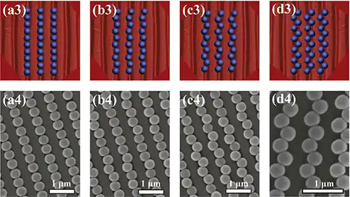
The influence of patterned surfaces on the formation of one- and two-dimensional colloidal crystals is analyzed. We have used the corrugated surface of a digital versatile disc (DVD) for template surface processing. When the sphere diameter is on the order of the groove width of patterned substrates, a rich variety of particle decorations appear. However, if particle size is much larger than template patterns, large domains of particle ordering are formed.

This paper investigates the sequence of morphological transitions in a nearly hard particle arrangement of colloidal crystals confined in a wedge cell. Earlier studies have shown intermediate particle arrangements (such as the buckling, rhombic, prismatic, and hcp like phases) to account for the drastic changes in the filling fraction values between the triangular and square arrangements. However, to the best of our knowledge, there is no complete description of the transitions between n and n + 1 layers. Here we describe the ordering of the particles for films between 1 and 4 layers. We also present a new intermediate phase hcp(011) to show the transition between nSQUARE, nTRIANGULAR for n > 2 layers.