Research · Publication & note
Multi-Mode Interference Revealed by Two-Photon Absorption in Silicon-Rich SiO₂ Waveguides - Notes

Research article
Published abstract
Photoluminescence (PL) from Si nanocrystals (NCs) excited by two-photon absorption (TPA) has been observed in Si nanocrystal-based waveguides fabricated by plasma enhanced chemical vapor deposition. The TPA excited photoluminescence emission resembles the one-photon excited photoluminescence arising from inter-band transitions in the quantum confined Si nanocrystals. By measuring the non-linear transmission of waveguides, a large TPA coefficient of β up to 10⁻⁸ cm/W has been measured at 1550 nm. These values of β depend on the Si NCs size and are two orders of magnitude larger than the bulk silicon value. Here, we propose to use the TPA excited visible PL emission as a tool to map the spatial intensity profile of the 1550 nm propagating optical modes in multimode waveguides. In this way, multimode interference has been revealed experimentally and confirmed through a finite elements simulation.
Article access and reuse
The supplied AIP published PDF is used locally for verification. No PDF or extracted figures are republished because this 2015 article does not display an open reuse licence. Consult the official AIP record and permissions policy. Official AIP Publishing article record · Rights and permissions.
Related publications


Research fields
Top-down
Silicon-rich SiO₂ is patterned into multimode channel waveguides whose width and composition set the supported transverse modes. The structures convert an otherwise hidden near-infrared interference pattern into visible nanocrystal luminescence.
Simulations & fits
Finite-element propagation calculations predict the modal beat lengths, while Fourier analysis extracts the corresponding spatial frequencies from the measured emission. Nonlinear transmission fits also determine the two-photon-absorption coefficient of each material composition.
Characterization
A picosecond 1550-nm pump excites visible photoluminescence through two-photon absorption along the waveguide. Imaging this emission from above directly maps multimode self-imaging and permits comparison of beat periods across widths that are difficult to probe from end transmission alone.
RESEARCH TOPICS
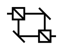 InterferenceThe interference pattern is not reconstructed from a conventional near-field scan. The spatial modulation observed along the 5 and 10 μm waveguides agrees with finite-element calculations, providing a direct experimental image of multimode beating.
 MaterialsThe active core is silicon-rich SiO₂ containing nanocrystals formed after deposition and thermal treatment. Its two-photon-absorption coefficient at 1550 nm reaches roughly 10⁻⁸-10⁻⁹ cm W⁻¹, more than an order above bulk silicon, which makes the otherwise invisible infrared field observable through visible nanocrystal luminescence.
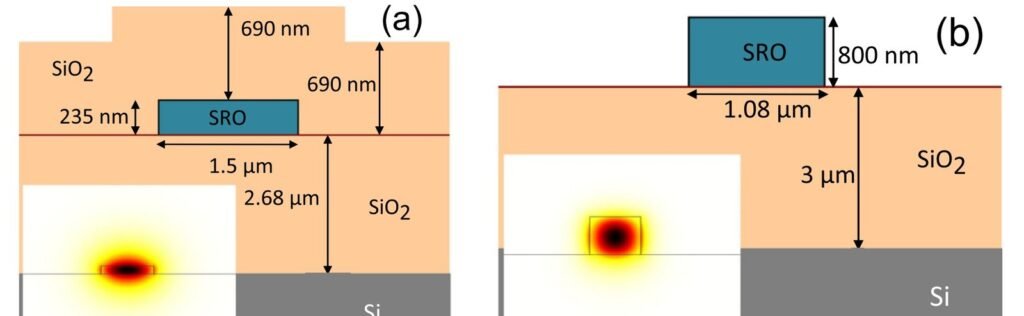
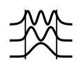 MultimodeFinite-element simulations classify the 1.5 μm guide as single-mode and the 5-10 μm guides as multimode at 1550 nm. The longitudinal bright-dark sequence is therefore tied to interference among guided modes rather than to random variations in nanocrystal concentration.
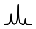 NonlinearThe resulting visible photoluminescence has the same spectral character as one-photon-excited emission, but its quadratic dependence on local intensity turns it into a sensitive nonlinear probe. The extracted imaginary third-order susceptibility is of order 10⁻¹²-10⁻¹⁴ cm² W⁻¹.