Research · Publication & note
La nanofotonica in silicio e la fotonica con il nanosilicio: una piattaforma per ampliare il successo della fotonica in silicio - Notes

Il Nuovo Saggiatore · Journal article · 2012
Published abstract
La fotonica integrata in silicio ha permesso di realizzare reti ottiche integrate in pochi mm² con velocità di trasmissione dati di più di 1 Tbps. Per poterne ampliare ulteriormente lo spettro di funzionalità ed applicazioni, a Trento applichiamo il paradigma delle nanotecnologie. Grazie alle nuove proprietà risultanti dal confinamento spaziale di portatori di carica (Nanosilicio) e di fotoni (Nanofotonica), abbiamo dimostrato una serie di funzionalità aggiuntive alla fotonica in silicio. Queste hanno permesso di realizzare amplificatori ottici, risonatori ottici, diodi elettroluminescenti, celle solari a resa elevata, biosensori biocompatibili e biodegradabili, interruttori tutti ottici superveloci, nodi di reti ultradensi, instradatori interferometrici, ed altro ancora.
How to cite
Article access and reuse
Società Italiana di Fisica permits authors to self-archive the accepted manuscript on their own website and allows repository availability after the stated embargo, but it does not permit public posting of the publisher's final version. The local file is the typeset publisher version, so neither that PDF nor its figures are hosted or reproduced here. Use the official record and the journal link for access.
Related publications





Research fields
Bottom-up
The article presents silicon nanocrystals and silicon colloids as material routes that introduce electronic or photonic confinement beyond bulk crystalline silicon. Deposition, annealing and particle formation are connected with room-temperature emission and wavelength-scale scattering.
Top-down
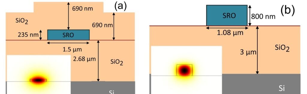
Planar waveguides, microcavities and resonators show how nanosilicon can be incorporated into silicon-photonic circuits. Device geometry supplies optical confinement while the nanostructured material adds emission or nonlinear functionality unavailable from passive bulk silicon alone.
RESEARCH TOPICS
 CouplingThe review uses SCISSOR chains (side-coupled sequences of ring resonators) to show how weak exchange between each ring and a common guide can build a collective spectral response. Coupling is presented as a circuit-design variable that connects isolated high-Q cavities into a functional filter rather than merely as an insertion loss.
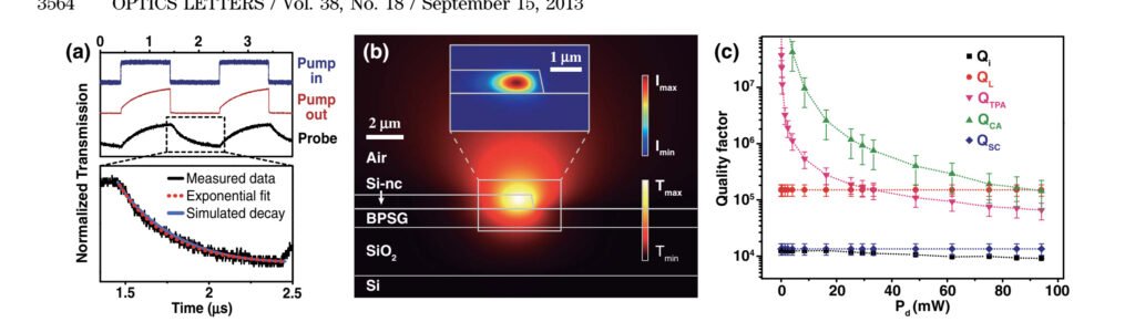
 EmissionSilicon nanocrystals overcome part of bulk silicon's poor radiative efficiency through quantum confinement, producing room-temperature visible photoluminescence. Emission is therefore discussed from both the material side and the cavity-filtering side.
 InterferenceThe review also explains how an optically induced nonlinear phase shift can switch an interferometer between those conditions. These examples connect the abstract idea of interference to concrete silicon circuits for filtering and all-optical routing.
 MaterialsNanosilicon supplies luminescence and a sizeable third-order response while remaining compatible with established microelectronic processing. Presenting both useful optical properties and degradation mechanisms avoids treating “silicon photonics” as a single ideal material and shows why composition, confinement and surface chemistry matter.
 MultimodeMicrodisks support many azimuthal whispering-gallery resonances, while coupled-ring chains create additional collective supermodes. Their narrow spectral spacing enables dense wavelength routing but also means that modal alignment, family selection and fabrication dispersion must be controlled.
 NonlinearSilicon nanocrystal composites are highlighted because their nonlinear response can enable fast all-optical switching at telecommunication wavelengths. Nonlinearity is therefore framed both as a switching resource and as a dynamical constraint in densely integrated cavities.
 QuantumQuantum confinement in nanometre-scale silicon changes the electronic density of states and relaxes the restrictions that make bulk silicon an inefficient light emitter. The discussion stays at the material-physics level: it does not claim single-photon operation, but explains how confinement provides optical functionality that ordinary crystalline silicon lacks.
 ResonatorsWhispering-gallery microdisks store light around their perimeter and imprint narrow resonances on the broad nanocrystal luminescence. The review uses this progression from one emitting disk to interconnected SCISSOR circuits to illustrate how resonators bridge material research and scalable silicon-photonic systems.