Research · Publication & note
Scanning Photocurrent Microscopy in Single Crystal Multidimensional Hybrid Lead Bromide Perovskites - Notes
Journal article
Published abstract
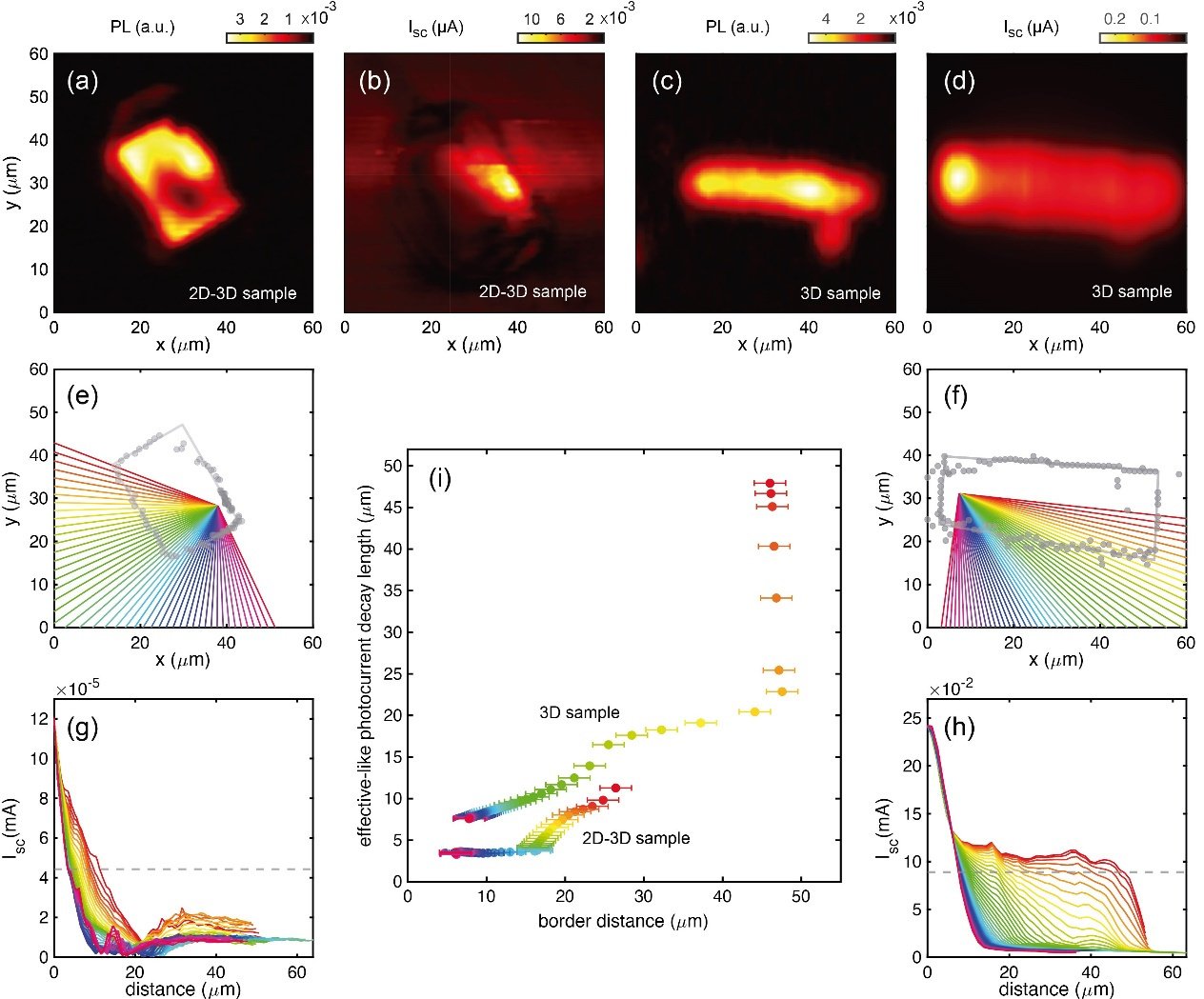
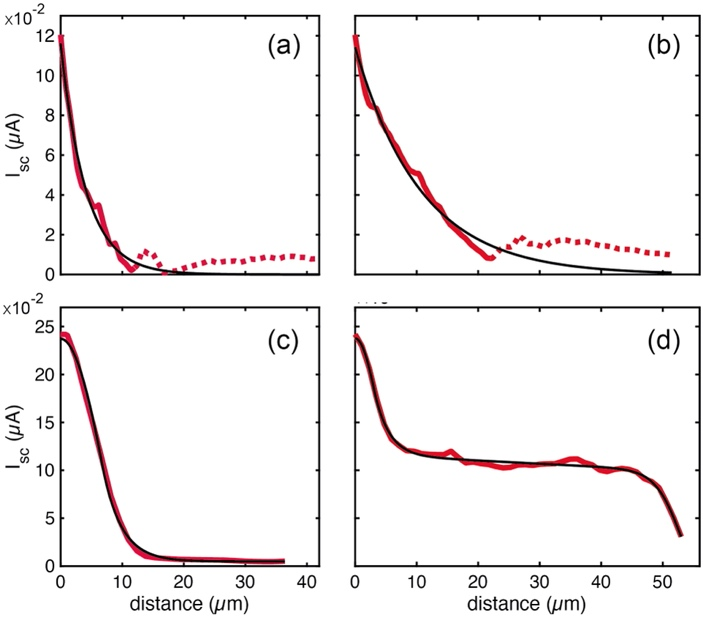
We investigated solution-grown single crystals of multidimensional 2D-3D hybrid lead bromide perovskites using spatially resolved photocurrent and photoluminescence. Scanning photocurrent microscopy (SPCM) measurements where the electrodes consisted of a dip probe contact and a back contact. The crystals revealed significant differences between 3D and multidimensional 2D-3D perovskites under biased detection, not only in terms of photocarrier decay length values but also in the spatial dynamics across the crystal. In general, the photocurrent maps indicate that the closer the border proximity, the shorter the effective decay length, thus suggesting a determinant role of the border recombination centers in monocrystalline samples. In this case, multidimensional 2D-3D perovskites exhibited a simple fitting model consisting of a single exponential, while 3D perovskites demonstrated two distinct charge carrier migration dynamics within the crystal: fast and slow. Although the first one matches that of the 2D-3D perovskite, the long decay of the 3D sample exhibits a value two orders of magnitude larger. This difference could be attributed to the presence of interlayer screening and a larger exciton binding energy of the multidimensional 2D-3D perovskites with respect to their 3D counterparts.
Figures
Source: E. Segura-Sanchis et al., Nanomaterials 13, 2570 (2023), CC BY 4.0.
Source: E. Segura-Sanchis et al., Nanomaterials 13, 2570 (2023), CC BY 4.0.
Source: E. Segura-Sanchis et al., Nanomaterials 13, 2570 (2023), CC BY 4.0.
Source: E. Segura-Sanchis et al., Nanomaterials 13, 2570 (2023), CC BY 4.0.
Source: E. Segura-Sanchis et al., Nanomaterials 13, 2570 (2023), CC BY 4.0.
Source: E. Segura-Sanchis et al., Nanomaterials 13, 2570 (2023), CC BY 4.0.
How to cite
Article access and reuse
This open-access article is distributed under the Creative Commons Attribution 4.0 licence; the journal version is the authoritative record. Official MDPI article record · CC BY 4.0 licence · MDPI rights and permissions.
Related publications
Research fields
Bottom-up
Solution-grown single crystals provide matched three-dimensional and multidimensional 2D-3D lead-bromide perovskites. Controlling the incorporated organic cation changes the layered character while retaining crystals large enough for spatially resolved transport measurements.
Simulations & fits
Photocurrent decay away from the probe is analysed with exponential transport models. A single regime describes the multidimensional crystals, whereas the 3D material requires fast and slow components, exposing a long-range contribution that differs by roughly two orders of magnitude.
Characterization
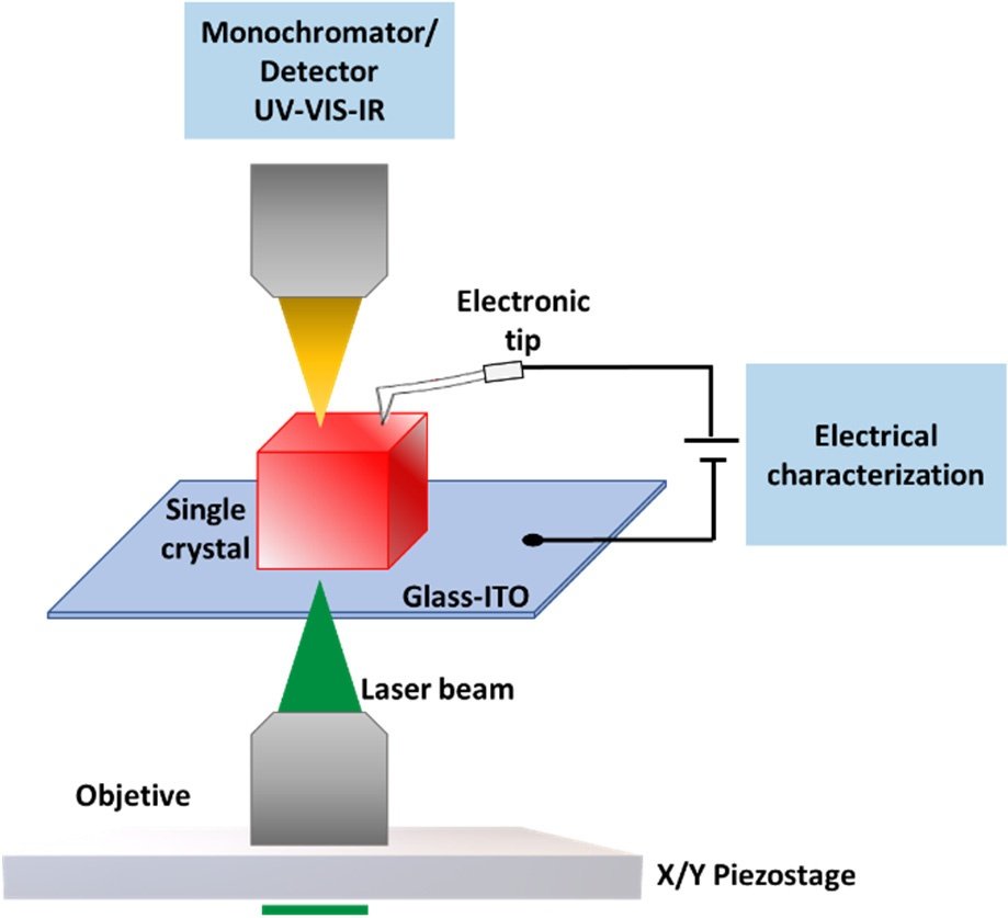
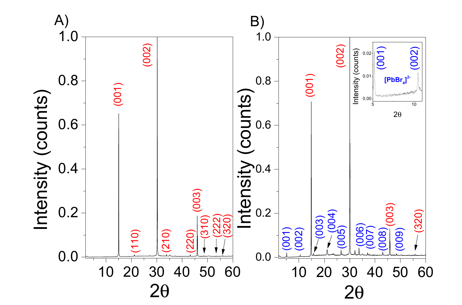
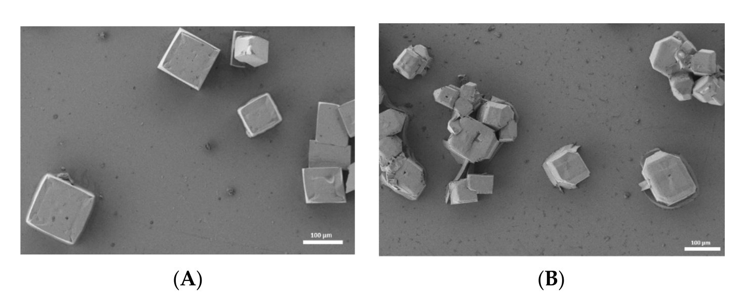
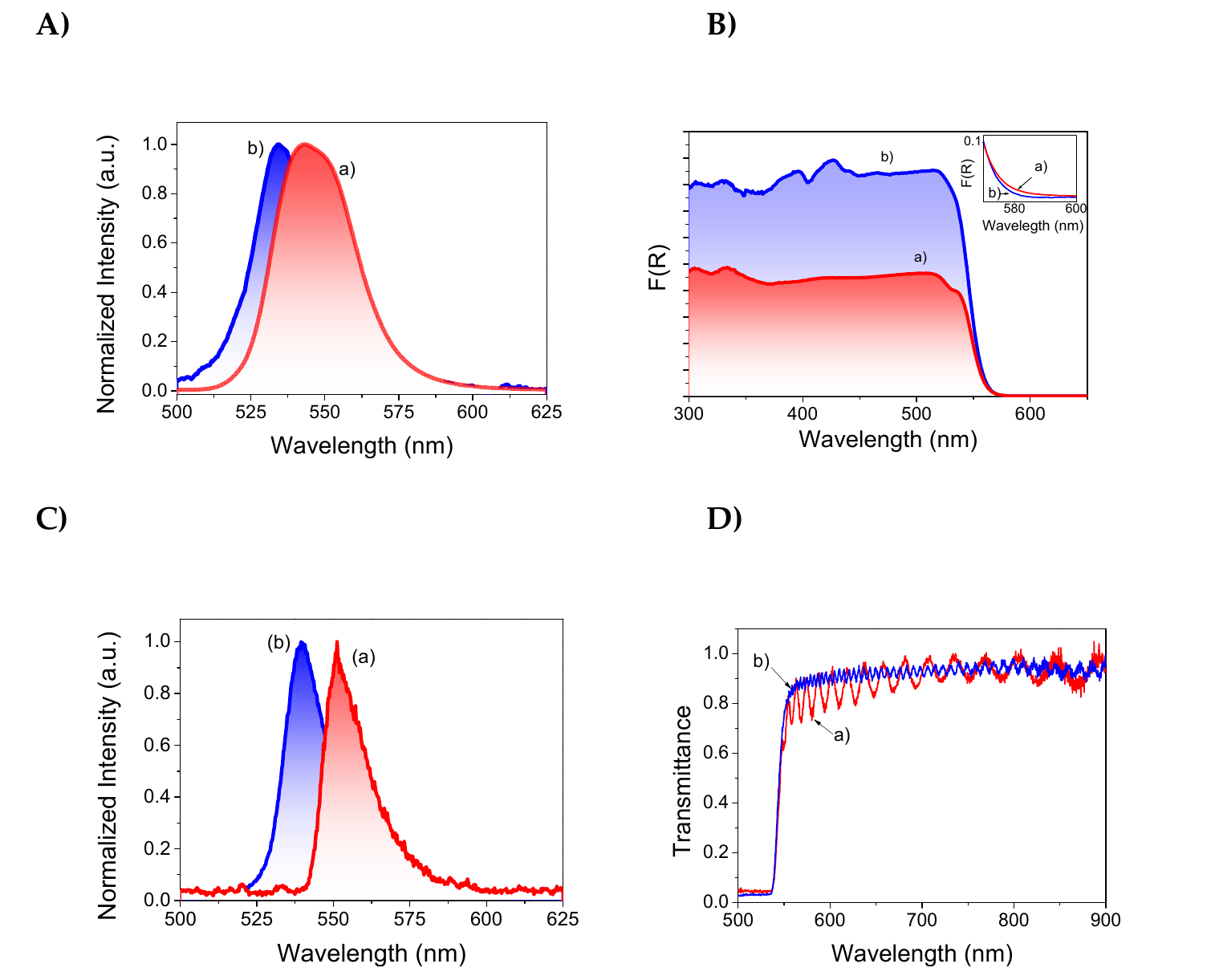
Scanning photocurrent microscopy with a movable tip and back contact maps charge collection across individual crystals. Photoluminescence, diffuse reflectance, X-ray diffraction and electron microscopy provide the optical, structural and morphological context needed to interpret border recombination and dimensionality-dependent transport.
RESEARCH TOPICS
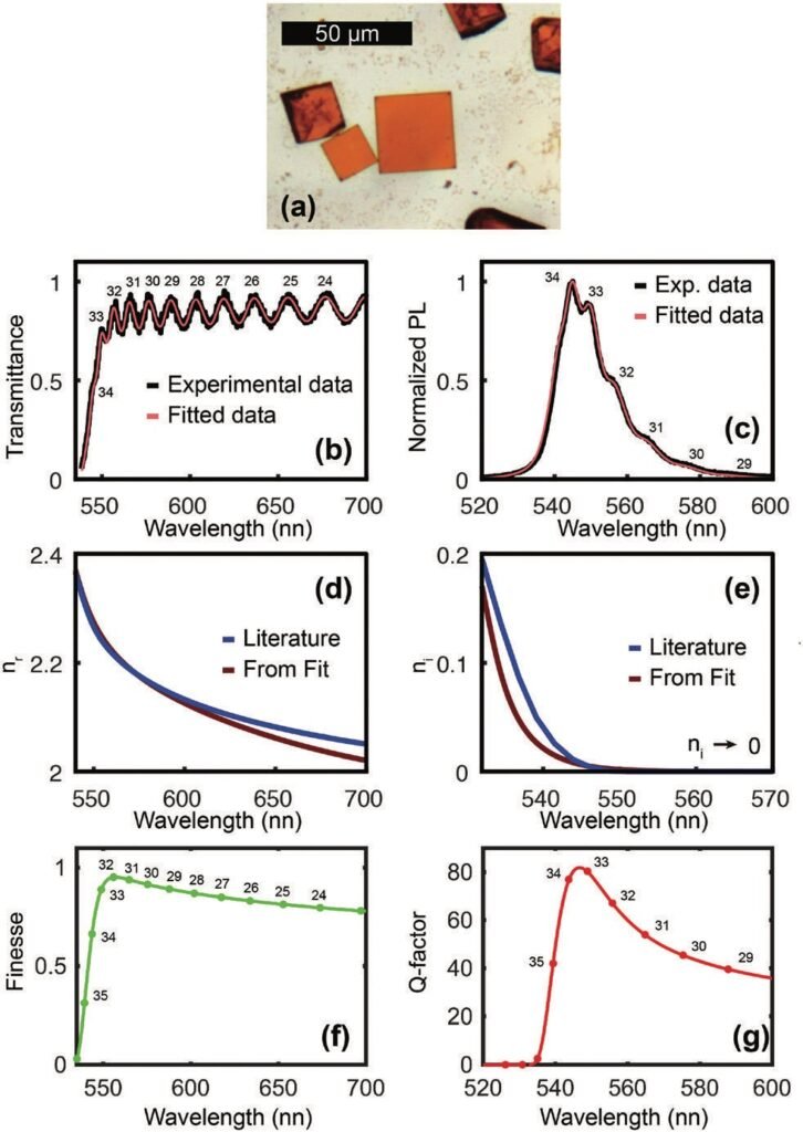
 EmissionThe optical comparison begins with spectra measured on both polycrystalline films and selected single crystals. Time-resolved measurements add a second distinction: the carrier lifetime is 9.70 ns in the 3D crystal and 18.39 ns in the 2D-3D crystal, showing that a longer luminescence lifetime does not by itself imply more efficient photocurrent collection.
 HarvestingThe key comparison is spatial rather than purely spectral. The 3D crystal requires an additional long-decay component, D2 = 328.88 ± 13.73 μm, which the authors identify as a possible fingerprint of its more efficient charge harvesting.
 MaterialsThe experiment separates two bromide perovskites whose dimensionality is changed through the organic cation: a conventional three-dimensional lattice and a mixed 2D-3D structure. Their different charge-transport profiles are therefore interpreted in relation to interlayer screening and the higher exciton binding energy expected in the multidimensional crystal.
 SetupsScanning photocurrent microscopy is performed on a single crystal placed on ITO-coated glass, which acts as the back electrode, while a movable conductive probe provides the local collecting contact. Recording photoluminescence and short-circuit current over the same area makes it possible to compare where light is emitted with where photogenerated carriers are actually collected; Figures 5 and 6 then relate those maps to profiles taken at controlled distances from the crystal edges.
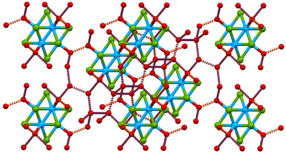
 ChemistryBoth materials are lead-bromide hybrid perovskites, but the organic-cation formulation changes how the inorganic framework is connected. The resulting contrast can therefore be discussed in terms of dimensionality, carrier binding and interlayer transport rather than only sample ageing.