Research · Publication & note
Groove-Assisted Solution Growth of Lead Bromide Perovskite Aligned Nanowires: A Simple Method towards Photoluminescent Materials with Guiding Light Properties - Notes
Journal article
Published abstract
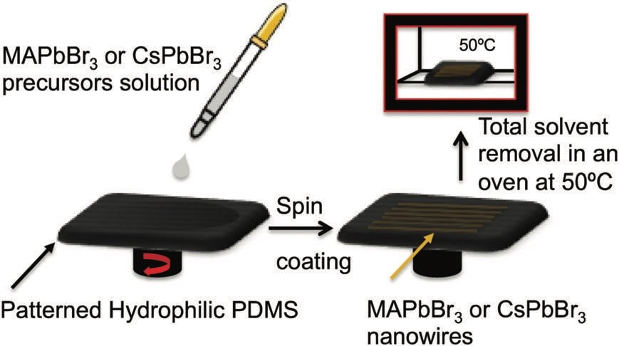
High refractive index nanowires are very attractive because of their waveguiding properties and their multiple applications. In this sense, metal halide perovskites, an emerging and appealing optoelectronic material, have also been tailored into nanowire structures. Here, we present an easy, low-cost and versatile method that has made possible to achieve nanowires of controlled and uniform width. The method has been applied here to all-inorganic and hybrid lead bromide perovskite (CsPbBr₃ and CH₃NH₃PbBr₃ respectively) materials. The procedure is based on the spin coating of precursors solutions, at room temperature, on a PDMS replica of the periodic grooves and lands of commercially available Compact Disc (CD) or Digital Versatile Disc (DVD) polycarbonate plates. The method can be applied for the synthesis of other material nanowires before being transferred onto other substrates. The obtained CsPbBr₃ and CH₃NH₃PbBr₃ nanowires exhibit high photoluminescence and guiding light properties along the material.
Figures
© 2019 The Royal Society of Chemistry and the Chinese Chemical Society. Source: I. Rodriguez et al., Materials Chemistry Frontiers 3(9), 1754-1760 (2019), DOI 10.1039/C9QM00210C. Reproduced by the authors in accordance with RSC author reuse rights.
© 2019 The Royal Society of Chemistry and the Chinese Chemical Society. Source: I. Rodriguez et al., Materials Chemistry Frontiers 3(9), 1754-1760 (2019), DOI 10.1039/C9QM00210C. Reproduced by the authors in accordance with RSC author reuse rights.
© 2019 The Royal Society of Chemistry and the Chinese Chemical Society. Source: I. Rodriguez et al., Materials Chemistry Frontiers 3(9), 1754-1760 (2019), DOI 10.1039/C9QM00210C. Reproduced by the authors in accordance with RSC author reuse rights.
© 2019 The Royal Society of Chemistry and the Chinese Chemical Society. Source: I. Rodriguez et al., Materials Chemistry Frontiers 3(9), 1754-1760 (2019), DOI 10.1039/C9QM00210C. Reproduced by the authors in accordance with RSC author reuse rights.
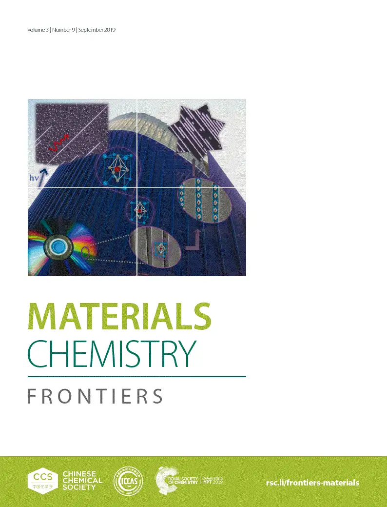
© 2019 The Royal Society of Chemistry and the Chinese Chemical Society. Article: I. Rodriguez et al., Materials Chemistry Frontiers 3(9), 1754-1760 (2019), DOI 10.1039/C9QM00210C. Reproduced by the authors with acknowledgement.
How to cite
Article access and reuse
The Version of Record is available from the Royal Society of Chemistry and is not hosted on this website. RSC authors retain the right to reuse their own figures in later publications and on personal websites when the original article is properly acknowledged. The four figures below are complete, unmodified compositions extracted from the article PDF.
Related publications
Research fields
Bottom-up
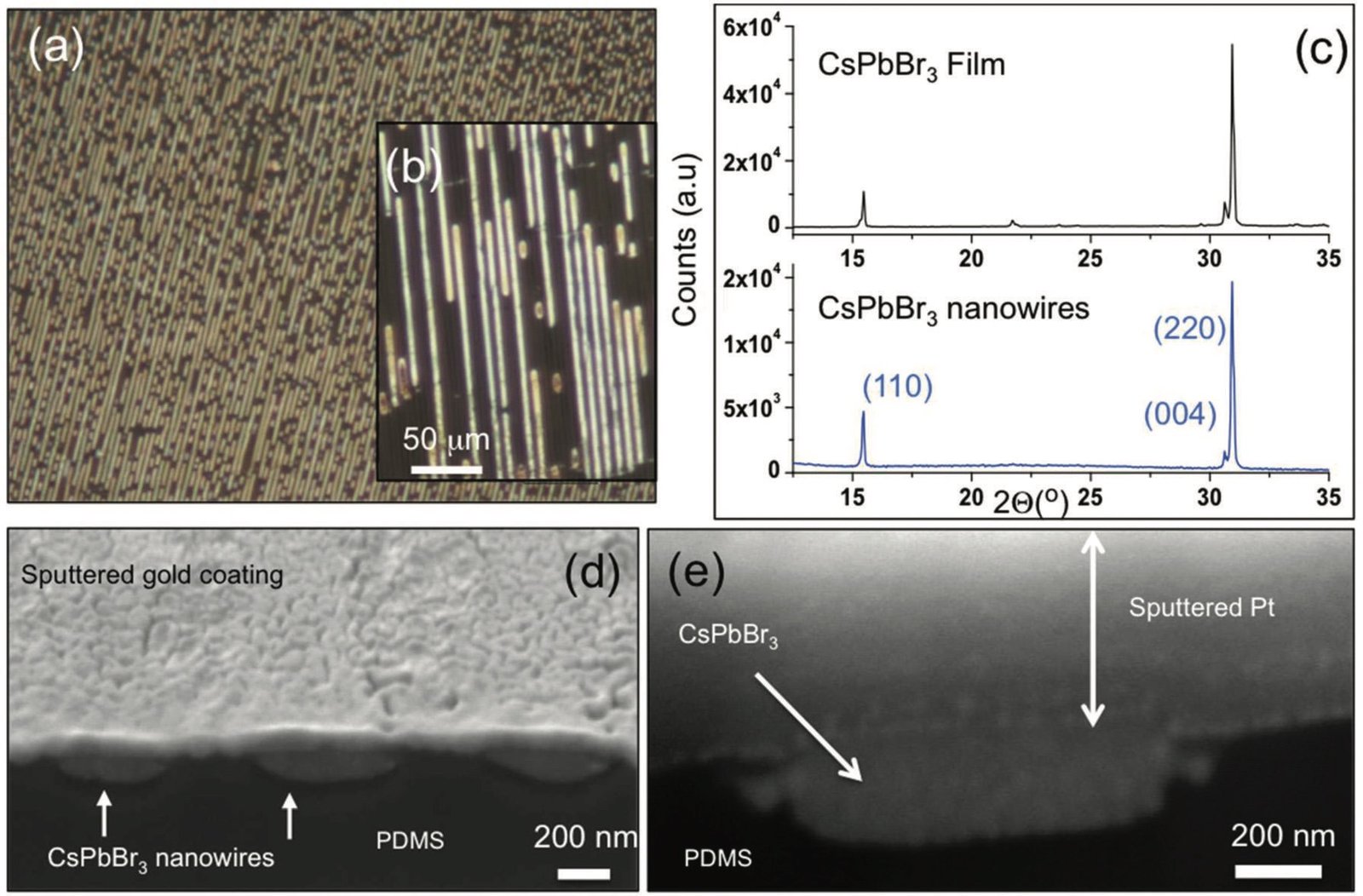
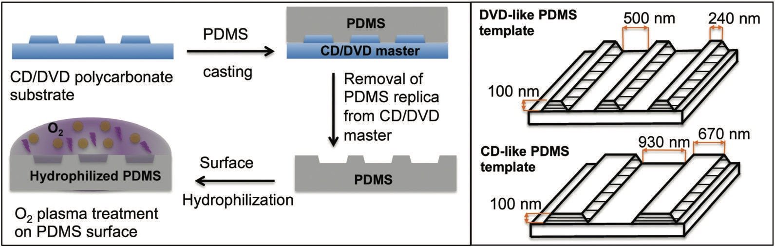
Perovskite precursor solutions crystallise inside submicrometre grooves replicated from commercial CD and DVD surfaces into PDMS. Confinement guides the room-temperature growth of aligned CsPbBr₃ and MAPbBr₃ nanowire arrays with dimensions set by the template profile.
Characterization
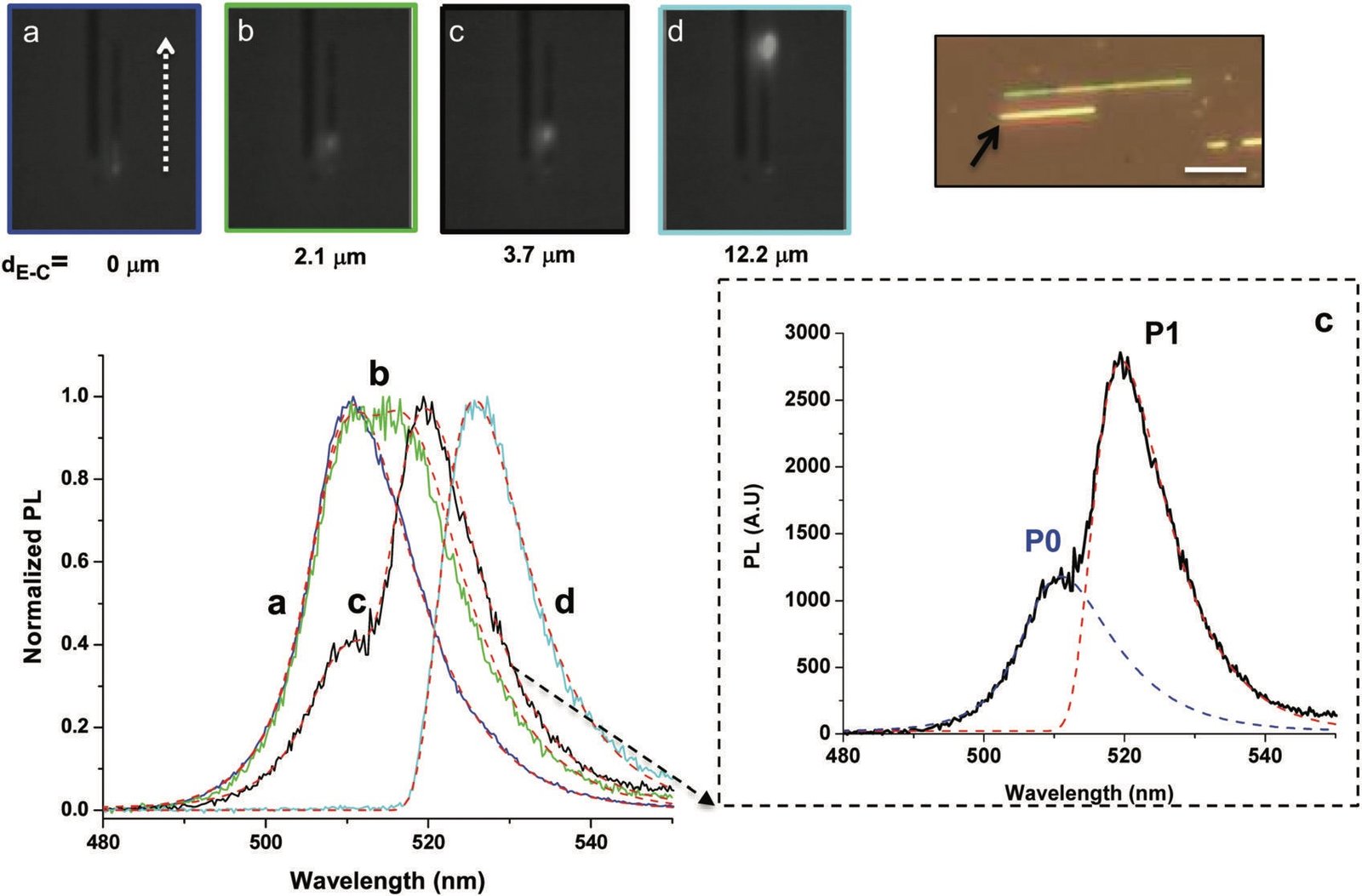
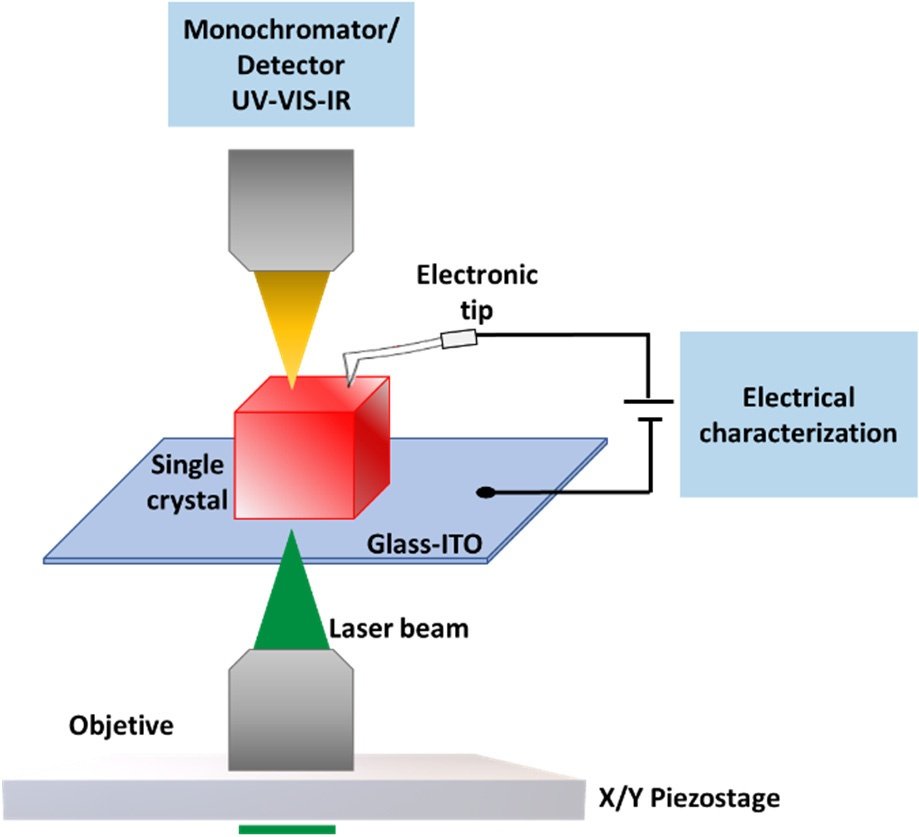
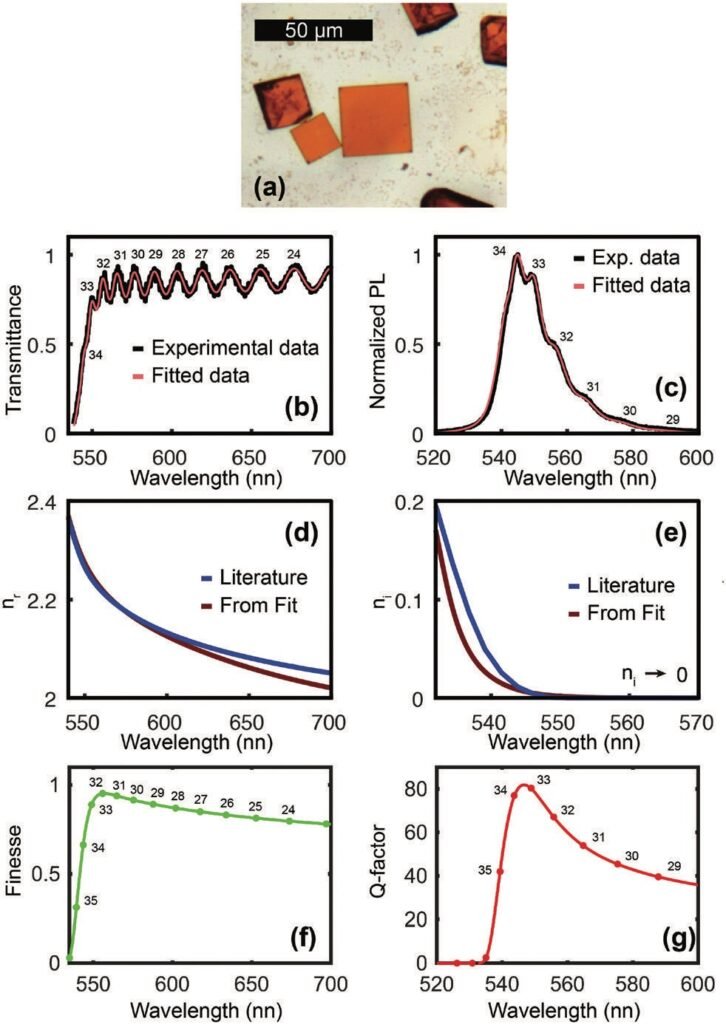
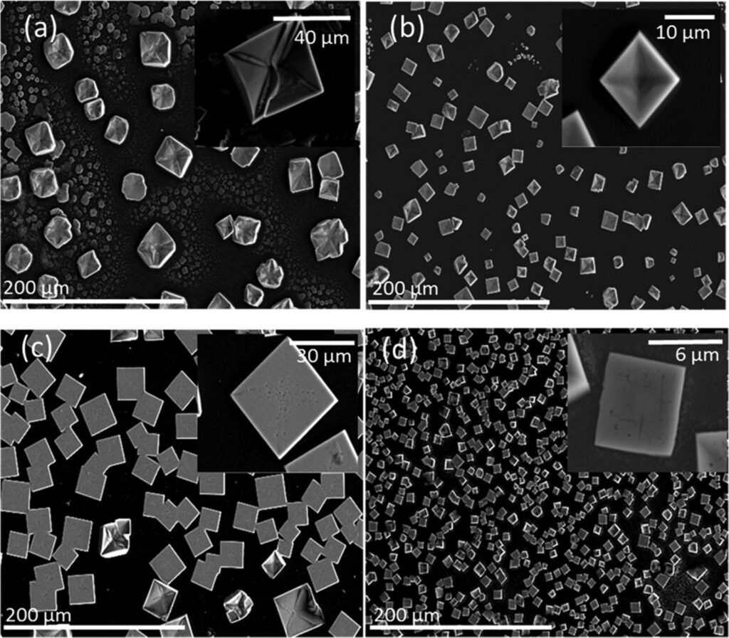
Optical microscopy, X-ray diffraction and FIB-assisted cross-sectional electron microscopy establish the nanowire alignment, phase and geometry. Spatial photoluminescence measurements then show that excitation can be guided along an individual wire, relating its crystal morphology to light transport.
RESEARCH TOPICS
 EmissionThe nanowires act as both emitters and waveguides. The decomposition shown with the optical measurements distinguishes local emission from guided light and explains why the remote spectrum changes shape rather than merely becoming weaker.
 MaterialsThe method is demonstrated with both all-inorganic CsPbBr3 and hybrid CH3NH3PbBr3, producing aligned polycrystalline wires whose width is imposed by a mould rather than only by a crystal growth direction. Because CD and DVD masters have different pitches and groove dimensions, the same low-cost process provides two controlled wire geometries and can be transferred to other solution-processed materials.
 ChemistryPDMS replicas are cast from the periodic grooves and lands of commercial CDs or DVDs, then spin-coated at room temperature with the appropriate lead-bromide perovskite precursor. This links solution chemistry directly to the final one-dimensional optical geometry.