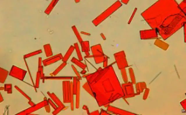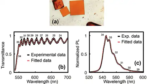


A precise knowledge of the optical properties, specifically the refractive index, of organic/inorganic perovskites, is essential for pushing forward the performance of the current photovoltaic devices that are being developed from these materials. Here we show a robust method for determining the real and the imaginary part of the refractive index of MAPbBr3 thin films and micrometer size single crystals with planar geometry. The simultaneous fit of both the optical transmittance and the photoluminescence spectra to theoretical models defines unambiguously the refractive index and the crystal thickness. Because the method relies on the optical resonance phenomenon occurring in these microstructures, it can be used to further develop optical microcavities from perovskites or from other optical materials.

High refractive index nanowires are very attractive because of their waveguiding properties and their multiple applications. In this sense, metal halide perovskites, an emerging and appealing optoelectronic material, have also been tailored into nanowire structures. Here, we present an easy, low-cost and versatile method that has made possible to achieve nanowires of controlled and uniform width. The method has been applied here to all-inorganic and hybrid lead bromide perovskite (CsPbBr3 and CH3NH3PbBr3 respectively) materials. The procedure is based on the spin coating of precursor solutions, at room temperature, on a PDMS replica of the periodic grooves and lands of commercially available Compact Disc (CD) or Digital Versatile Disc (DVD) polycarbonate plates. The method can be applied for the synthesis of other material nanowires before being transferred onto other substrates. The obtained CsPbBr3 and CH3NH3PbBr3 nanowires exhibit high photoluminescence and guiding light properties along the material.