Research · Publication & note
Monolayer-to-Mesoscale Modulation of the Optical Properties in 2D CrI3 Mapped by Hyperspectral Microscopy - Notes
Research article
Published abstract
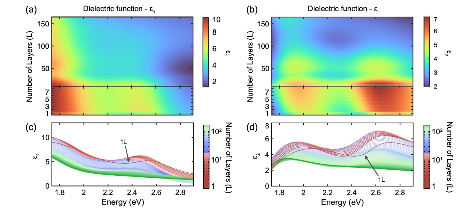
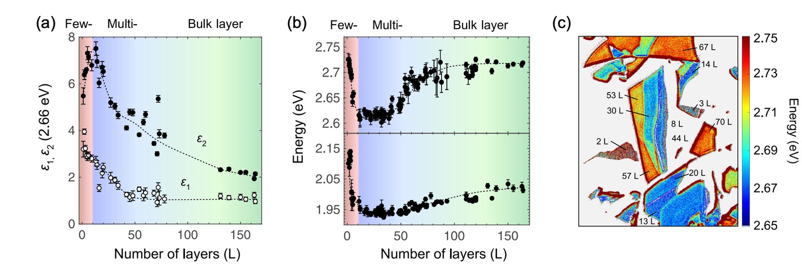
Magnetic 2D materials hold promise to change the miniaturization paradigm of unidirectional photonic components. However, the integration of these materials in devices hinges on the accurate determination of the optical properties down to the monolayer limit, which is still missing. By using hyperspectral wide-field imaging at room temperature, we reveal a nonmonotonic thickness dependence of the complex optical dielectric function in the archetypal magnetic 2D material CrI₃ extending across different length scales: onsetting at the mesoscale, peaking at the nanoscale, and decreasing again down to the single layer. These results portray a modification of the electronic properties of the material and align with the layer-dependent magnetism in CrI₃, shedding light on the long-standing structural conundrum in this material. The unique modulation of the complex dielectric function from the monolayer up to more than 100 layers will be instrumental for understanding mesoscopic effects in layered materials and tuning light-matter interactions in magnetic 2D materials.
Figures
Source: M. Galbiati et al., Physical Review Letters 130, 176901 (2023); author personal website.
Source: M. Galbiati et al., Physical Review Letters 130, 176901 (2023); author personal website.
Source: M. Galbiati et al., Physical Review Letters 130, 176901 (2023); author personal website.
Source: M. Galbiati et al., Physical Review Letters 130, 176901 (2023); author personal website.
Article access and reuse
APS permits authors to reuse material from their articles on a personal website with proper citation. The Version of Record remains authoritative. Official article record · APS copyright and permissions policy.
Related publications
Research fields
Simulations & fits
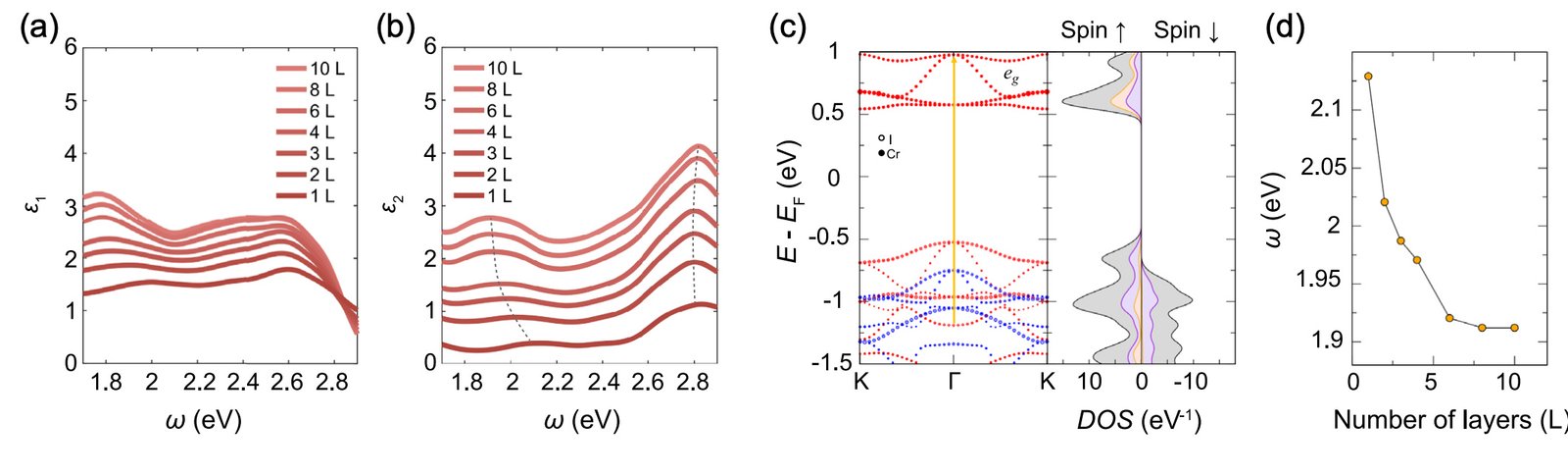
A multilayer Fabry-Pérot model and a two-oscillator dielectric function are fitted simultaneously to hyperspectral transmittance data from different CrI₃ thicknesses. First-principles calculations then relate the observed dielectric evolution to changes in the layer-dependent electronic structure.
Characterization
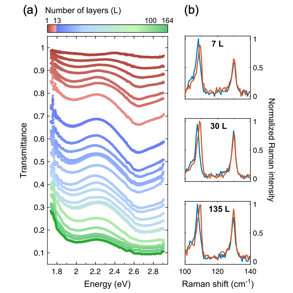
Hyperspectral microscopy maps transmittance from the monolayer to mesoscale thicknesses on the same exfoliated CrI₃ flake. The spatially registered spectra separate few-layer, multilayer and bulk-like regimes and show that the monolayer optical response is not a simple thin limit of the bulk material.
RESEARCH TOPICS
 MagnetismCrI3 changes its magnetic ordering with thickness: few-layer samples are layered antiferromagnets, whereas the bulk is ferromagnetic, with the crossover occurring in the tens-of-nanometres range. The hyperspectral measurements reveal an optical crossover at a comparable mesoscale thickness.
 MaterialsThe complex dielectric function is tracked continuously from a monolayer to flakes containing more than 100 layers. AFM and Raman checks confirm that the exfoliated flakes are atomically flat and chemically pristine, reducing thickness errors and degradation as alternative explanations.
 QuantumThe optical trend is interpreted as a modification of CrI3's electronic structure, not merely as a classical interference artefact. This makes the thickness-dependent optical response relevant to quantum and spin-photonic devices in which magnetic order and light-matter interaction must be controlled together.
 SetupsWide-field hyperspectral microscopy records transmission over many pixels and wavelengths at room temperature, allowing dielectric properties to be mapped on mechanically exfoliated flakes too small for conventional ellipsometry. Figure 3 provides an internal cross-check: parameters extracted from the fit reproduce the independent evolution of the transmittance minima, while AFM supplies the layer thickness and Raman spectroscopy identifies the structural phase.